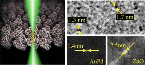
Aberration-Corrected Electron Beam Lithography at the One Nanometer Length Scale

Citation
Manfrinato, V.R.; Stein, A.; Zhang, L.; Nam, C.-Y.; Yager, K.G.; Stach, E.A.; Black, C.T. "Aberration-Corrected Electron Beam Lithography at the One Nanometer Length Scale"
Nano Letters 2017,
17 4562–4567.
doi: 10.1021/acs.nanolett.7b00514Summary
We demonstrate record-setting resolution for electron-beam patterning. In particular, we pattern at the <2 nm scale by using aberration-correcting optics.
Abstract
Patterning materials efficiently at the smallest length scales is a longstanding challenge in nanotechnology. Electron-beam lithography (EBL) is the primary method for patterning arbitrary features, but EBL has not reliably provided sub-4 nm patterns. The few competing techniques that have achieved this resolution are orders of magnitude slower than EBL. In this work, we employed an aberration-corrected scanning transmission electron microscope for lithography to achieve unprecedented resolution. Here we show aberration-corrected EBL at the one nanometer length scale using poly(methyl methacrylate) (PMMA) and have produced both the smallest isolated feature in any conventional resist (1.7 ± 0.5 nm) and the highest density patterns in PMMA (10.7 nm pitch for negative-tone and 17.5 nm pitch for positive-tone PMMA). We also demonstrate pattern transfer from the resist to semiconductor and metallic materials at the sub-5 nm scale. These results indicate that polymer-based nanofabrication can achieve feature sizes comparable to the Kuhn length of PMMA and ten times smaller than its radius of gyration. Use of aberration-corrected EBL will increase the resolution, speed, and complexity in nanomaterial fabrication.

